Current Mode DC/DC Converter Operation
Current Mode dc/dc Converter Operation
This article explains how a current mode dc/dc converter works. It explains how the feedback signal, error amplifier, current sense trip voltage and softstart all interplay to regulate the output voltage of a current mode dc/dc converter.
This is not just specific to current mode buck converters, although the examples used in this text are buck converters. Indeed it is applicable to all types of current mode converters including the SEPIC, Cuk, boost, buck-boost and flyback.
Figure 1 shows a basic current mode buck converter.
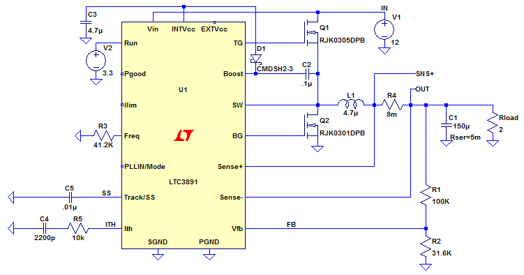
Figure 1
The Basics
Before discussing the error amplifier it is worth explaining the basic workings of a buck converter. On start up Q1 switches on, shorting the left hand side of the inductor to VIN. Current ramps linearly through the inductor until the voltage across the current sense resistor reaches a specific value (typically about 100mV). When the voltage across the current sense resistor reaches 100mV, Q1 switches off and Q2 switches on shorting the left hand side of the inductor to 0V. The inductor current continues to flow in the same direction, decreasing linearly and discharges into the output capacitor and load.
This is described in more detail in this article:
Buck Converter Design
The Error Amplifier
Figure 2 shows the internal workings of a typical current mode dc/dc converter.
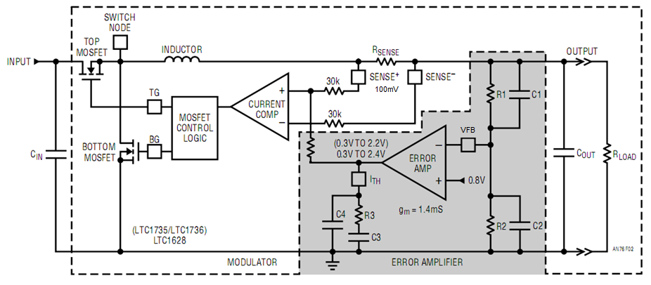
Figure 2
The feedback pin is connected to the inverting input of the error amplifier, so an increasing voltage on the feedback pin will create a decreasing voltage on the output of the error amplifier. The internal reference voltage, 0.8V, is connected to the non inverting input.
The output of the error amplifier controls the peak current through the inductor, by changing the current sense trip threshold (100mV). This pin is often called the ITH pin for Current (I) Threshold (TH).
On start up the output voltage is at 0V, so the feedback pin is at 0V. Since the feedback pin is connected to the inverting pin of the error amplifier, the output of the error amplifier is high (typically around 2.4V). As the output of the error amplifier controls the peak current in the inductor, a high voltage on the error amplifier output sets the current trip threshold at its maximum of 100mV. This ensures the maximum current flows in the inductor, hence the maximum current flows into the output capacitor, ensuring the output voltage is brought up to regulation as quickly as possible.
As the output voltage reaches regulation, the feedback pin is pulled up towards its regulation voltage, which is equal to the internal reference voltage (0.8V in Figure 1). An increasing voltage on the feedback pin reduces the voltage on the output of the error amplifier thus reducing the current sense trip threshold down from 100mV to, say, 50mV. This throttles back the peak inductor current, thus reducing the current flowing into the circuit and hence reducing the current flowing into the output capacitor. This provides a gentle top up of the output capacitor voltage and ensures the output capacitor does not overshoot.
If this mechanism were not in place and the current sense trip threshold remained at 100mV, too much inductor current would flow and when this current is dumped into the output capacitor, the output voltage would overshoot.
Thus the current mode buck converter reaches regulation.
Figure 3 shows a plot of Current Sense Voltage vs Error Amplifier Output Voltage. Ignoring light load conditions (when the part is in Burst Mode or Pulse Skipping), we can see that the relationship between the current sense voltage and the ITH voltage is linear.
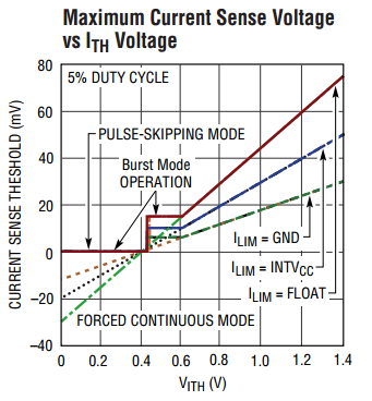
Figure 3
If a load is suddenly applied to the output, the output voltage dips, the feedback pin dips and the output of the error amplifier rises. This causes the current sense trip threshold to rise. The inductor now has a higher current trip threshold to ‘aim’ for, so the high side FET (Q1) switches on for longer. Thus the duty cycle momentarily increases. Thus more current flows in the inductor, so more current flows into the output capacitor and the output capacitor is topped up to its regulated voltage.
When the output capacitor is topped up, the feedback pin voltage increases causing the output of the error amplifier to decrease, the duty cycle decreases and the circuit goes back to steady state operation. Therefore the duty cycle before the load is applied is the same as the duty cycle after the load is applied. The duty cycle only increases for a few cycles at the moment the extra load is applied.
A subtle side effect of the high side FET switching on for a longer duration is that the low side FET switches on for a shorter duration, since the switching period is fixed. This means the inductor current has less time to decay, so the average inductor current is now at a higher value than before the load was applied. This higher average inductor current is now equal to the higher load current demanded by the newly applied load.
Thus the current mode dc/dc converter is effectively a voltage controlled current source. The ‘voltage’ is the output of the error amplifier and this is used to control the peak current flowing in the inductor by altering the current sense trip threshold. By varying the voltage on the output of the error amplifier, we can vary the peak inductor current.
But we need an output voltage, not an output current..?
The inductor current feeds into the load thus developing an output voltage and this output voltage is monitored by the error amplifier. A varying load, regardless of what it is, can be modelled as a varying resistor. However, fundamentally, the current mode dc/dc converter’s purpose is to generate an output current, not an output voltage. The output current is turned into an output voltage by the resistive load and this output voltage is monitored by the feedback resistors and error amplifier ensuring that, although the controller is outputting a current, it is the output voltage that is ultimately regulated.
With a voltage mode control converter, the controller changes the PWM duty cycle to regulate the output voltage. This duty cycle (at the junction of the two switching FETs) is smoothed by the output inductor and capacitor. This inductor/capacitor network has the potential to introduce a 180 degrees phase shift in the feedback loop which will make the controller go unstable. The main benefit of a current mode controller is that, because the controller is monitoring the inductor current, the phase shift introduced by the inductor is removed from the feedback loop. Therefore the only phase shift introduced is due to the output capacitor which is a maximum of 90 degrees, so well away from the point of instability.
Another benefit of current mode control is that a high current dc/dc converter can be constructed from multiple lower current dc/dc converters connected in parallel. As long as the feedback pins are connected together (so the same error signal is fed into each controller) and the ITH pins are connected together (so the same control signal is sent to the current sense voltage) the parts will share current.
Soft Start
Soft start is an integral part of the operation of the error amplifier. If the controller has soft start, at start up the output voltage regulates according to the voltage on the soft start capacitor and NOT the reference voltage. The soft start pin outputs a constant current, so by selecting a suitably sized soft start capacitor we can control the linear ramp on the soft start capacitor. If the controller regulates according to the voltage on the soft start capacitor, by selecting the correct soft start capacitor, we can control the ramp voltage on the output.
However, the soft start pin also controls the input current. By forcing the soft start voltage (which is our reference voltage at start up) to 0V, we can force the output of the error amplifier low on start up. A low voltage on the output of the error amplifier forces the current sense trip threshold low, thus reducing the peak inductor current to zero. Slowly ramping the soft start voltage slowly ramps up the voltage on the output of the error amplifier, so slowly ramps up the peak inductor current.
When the voltage on the soft start capacitor reaches the reference voltage, the reference voltage takes over and the part regulates according to the reference voltage.
So the soft start capacitor not only forces a ramp on the output voltage, it also ramps the peak inductor current, soft starting the input current.
Figure 4 shows a modified version of the circuit in Figure 1 to test the effect of forcing a voltage onto the output of the error amplifier as well as dumping a load on the output of the circuit once the circuit has reached regulation.
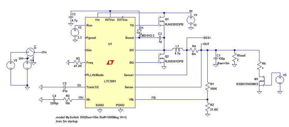
Figure 4
Running the simulation we can see that the output voltage rises linearly, controlled by the voltage on the soft start capacitor, as shown in Figure 5. Likewise the peak voltage across the current sense resistor rises linearly due to the action of the soft start capacitor.
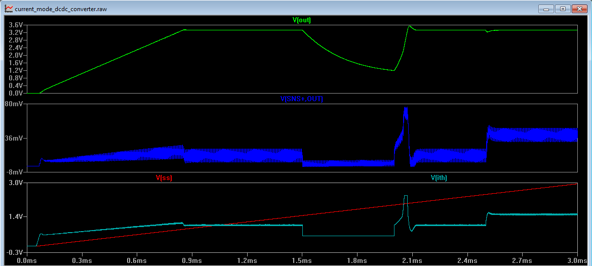
Figure 5
To test the effect of modulating the output of the error amplifier, the circuit in Figure 4 forces a voltage onto the ITH pin once the part has reached regulation.
Voltage V3 is set to 500mV. At 1.5ms, switch S1 closes thus clamping the ITH pin at 500mV. This clamps the maximum trip threshold across the current sense resistor, thus limiting the peak inductor current. Because the load is unchanged, the output voltage drops since less current is flowing into the circuit.
At 2ms the switch is opened and the circuit returns to regulation. However, since the circuit has finished its soft start routine, there is nothing limiting the output of the error amplifier, so the error amplifier voltage rises to its maximum value, so the current sense trip threshold is at its maximum. Thus a large current flows into the inductor and the output capacitor quickly rises to regulation, without the limitation of the soft start circuitry.
At 2.5ms, FET M1 is turned on, dumping a load on the output. The output voltage dips as does the voltage on the feedback pin. Therefore the output of the error amplifier rises, increasing the peak current sense trip threshold. The duty cycle increases for 3 cycles (shown in Figure 6), the inductor current increases, more current flows into the output capacitor and the output capacitor comes back to regulation.
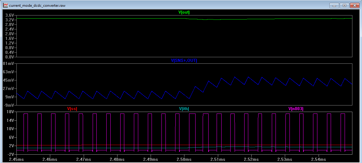
Figure 6
The LTspice simulation file can be downloaded here: Current Mode dc/dc converter
LTspice is a registered trademark of Analog Devices Inc
LTspice is a registered trademark of Analog Devices Inc
Sitemap: www.simonbramble.co.uk/sitemap
© Copyright Simon Bramble