LTspice Tutorial: Part 3
What we have learned so far enables us to simulate most designs. This LTspice Tutorial digs deeper into circuit analysis with LTspice®.
Figure 1 shows the jig of the LTC3878 external FET buck converter with a resistive load of 80mOhms. It can be downloaded here: LTC3878 buck converter
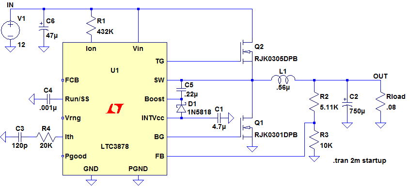
Figure 1
Running the simulation shows the output settles at 1.2V. Right click on the plot pane and select Add Plot Pane. In the schematic window hold down the ALT key and left click over the resistor Rload. This will plot the instantaneous power dissipation in the plot window as shown in Figure 2 with the units on the y axis.
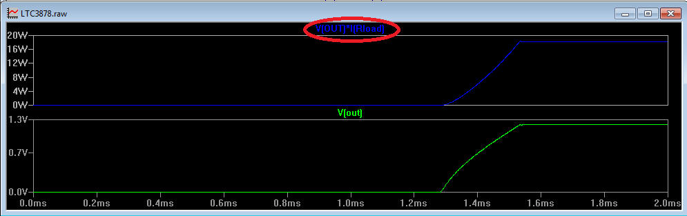
Figure 2
If it appears in the incorrect plot pane, left click on the plot icon and drag it to the correct pane.
In the plot window, hold down the CTRL key and left click over the plot icon (circled above in Figure 2) to bring up details of the average power dissipation, averaged over the time span of the plot. Selecting a section of the plot zooms in on the waveform and repeating CTRL left click shows the average power of that subsection of the waveform.
LTspice Tutorial 3: Generating the Efficiency Report
To generate an efficiency report, from the menu bar select Simulate -> Configure Analysis and select 'Stop simulating if steady state is detected'. Rerun the simulation. Then click on View -> Efficiency Report -> Show on Schematic. The efficiency report will appear on the schematic, as shown in Figure 3.
Note: the efficiency report can only be generated when there is only one voltage source (which is assumed to be the input) and either one current source or a load called Rload (which is assumed to be the load).

Figure 3
Repeating the above steps removes the efficiency report from the schematic.
It is also worthwhile returning to Simulate -> Configure Analysis and unchecking the box 'Stop Simulating if steady state is detected'
LTspice Tutorial 3: Using Maths functions to Calculate Efficiency
There is no reason why you cannot use the maths functions in LTspice to examine efficiency and indeed this is an effective way of measuring the efficiency of a multi output system.
A behavioral voltage source gives an output voltage according to a mathematical function. If we set up a behavioral voltage source to produce a voltage equal to the product of the input voltage and input current, we can then plot the input power over time. Likewise we can set up a behavioral voltage source to produce a voltage equal to the output powers of each converter. We can then set up a behavioral voltage source to produce a voltage equal to the ratio of output power to input power that then gives us a real time efficiency figure.
Consider the circuit in Figure 3a. This is a simple circuit consisting of two 5V linear regulators driven from a 10V input, each providing a load current of 10mA. B1 is a behavioral voltage source whose output voltage is equal to Vin * Iin. B5 and B2 produce voltages (P1 and P2) equal to the output powers of each regulator. B3 outputs a voltage equal to the function (100*(P1+P2)/Pin) - in other words the efficiency.
Setting up behavioral voltage sources can be tricky. It is best to construct the main circuit first, run the simulation, probe the desired voltages and currents and see what LTspice calls each voltage plot. The behavioral components need to correspond with these plot names.
The circuit of Figure 3a can be downloaded here: Behavioral Voltage Sources

Figure 3a
LTspice Tutorial 3: Simulating a Transient Load
We are now going to add a transient load to the output via a switch. Click the icon and select 'sw' and place the switch on the schematic. Add the extra load components as shown in Figure 4, including a PULSE voltage source transitioning from 0V to 5V at 1.7ms of duration 1ms to control the switch.
We are now going to add a transient load to the output via a switch. Click the
icon and select 'sw' and place the switch on the schematic. Add the extra load components as shown in Figure 4, including a PULSE voltage source transitioning from 0V to 5V at 1.7ms of duration 1ms to control the switch.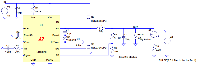
Figure 4
The switch now needs to be defined. The best way of defining a switch is to go into the help files (by hitting <F1>) and searching for 'switch', then selecting Voltage Controlled Switch. This will bring up the dialogue shown in Figure 5.
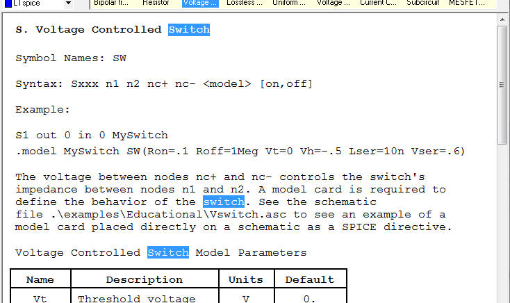
Figure 5
Highlight the line beginning '.model' and copy it. Back in the schematic editor, press the Spice Directive button and paste the text in as a Spice directive. Change the Spice directive to:
.model MySwitch SW(Ron=1m Roff=1Meg Vt=1)
to characterise the switch with an ON resistance of 1mOhm, an OFF resistance of 1MOhm and a threshold voltage of 1V. We don't need the other characteristics.
Place the text anywhere on the schematic.
To relate the switch to the .model we have just defined, right click on the switch symbol in the schematic window. In the Value field, enter MySwitch to relate the .model definition with the switch, as shown in Figure 6
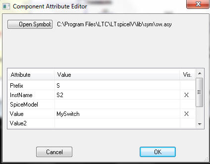
Figure 6
Run the simulation. The output voltage and current through the extra resistor should look like Figure 7.
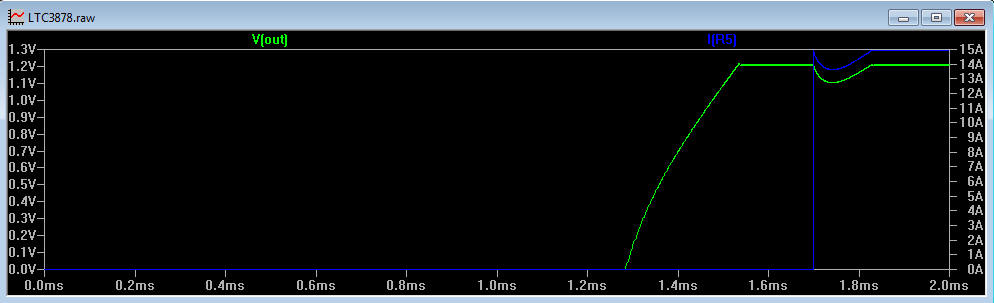
Figure 7
Now, the above simulation has been conducted with ideal components. This is normally quite acceptable until it comes to measuring the impact of the effective series resistance (ESR) of the output capacitor, C2. The circuit is designed to support a 15A load, so large current surges will be flowing from the inductor to the output capacitor and any ESR in C2 will manifest itself as ripple on the output voltage. With a 1.2V output, this ripple could quite easily violate the output specification.
Right clicking over capacitor C2 brings up the parameter table for the capacitor. We can either enter an ESR of our choice or we can press the Select Capacitor button to select one of the library capacitors in LTspice. LTspice contains libraries of many passive and active components and these can be selected by right clicking over the component of choice and browsing the libraries.
Running the simulation with an ESR of 0.5 Ohms shows the effect on the output voltage.
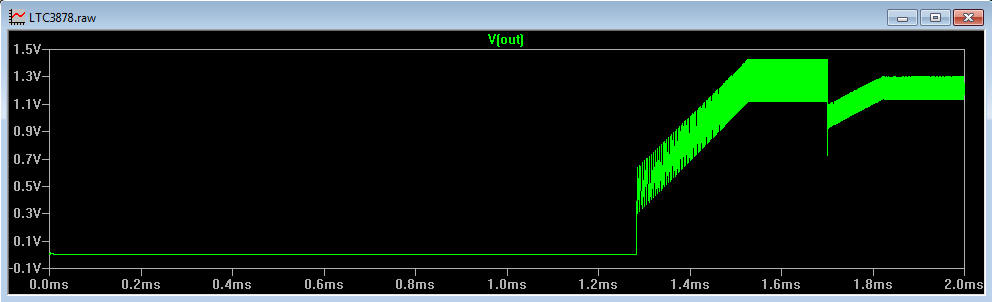
Figure 8
Right clicking over most passive components allows us to add parasitic elements or select from the component tables already stored in LTspice. On a note of design, if the ESR is a problem, adding several capacitors in parallel reduces the effective ESR. A simulation with 6x100uF capacitors, each with an ESR of 0.5Ohms reduced the ripple from 329mV to 170mV.
In the same way we can add a parasitic ESR to a capacitor, we can also add a series resistance to an inductor, just by right clicking over the inductor and entering a value in the Series Resistance box.
It is easy to lose track of what parasitics have been included in the circuit, so pressing <CTRL> <ALT><SHIFT> H highlights on the schematic what components have parasitic elements. Press <F9> to undo.
We are now going to look at simulating a transformer based design. Download the circuit in FIG 9: LTC3872 flyback converter
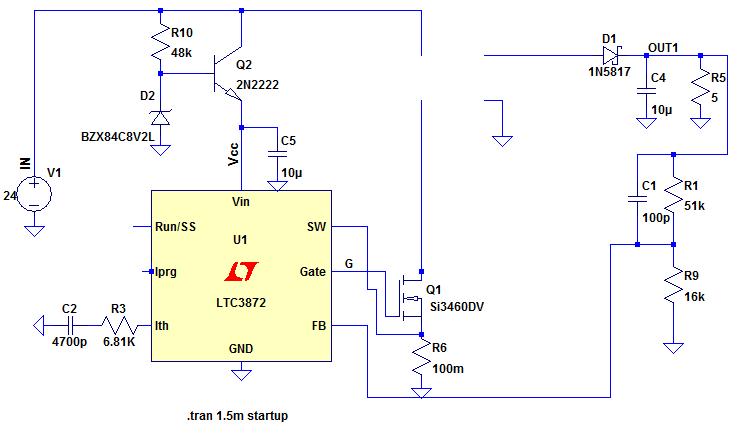
Figure 9
This missing transformer can be made up of 2 inductors, together with a SPICE directive coupling the inductors.
Insert an inductor of 50uH in the primary and 2uH in the secondary. To make the two inductors into a transformer, we need to tell LTspice that they are linked via a mutual inductance, K. Insert a SPICE directive using the button and insert the text
Insert an inductor of 50uH in the primary and 2uH in the secondary. To make the two inductors into a transformer, we need to tell LTspice that they are linked via a mutual inductance, K. Insert a SPICE directive using the
button and insert the textK1 L1 L2 1
This creates a mutual inductance, K1, between inductors L1 and L2 of value 1 (they have perfect coupling).
You will notice that the dots have been added to the transformer. Make sure they have the correct polarity for a flyback transformer. Change the value of the primary inductor to 50uH and the secondary inductor to 2uH.
You should now have a circuit similar to Figure 10
You will notice that the dots have been added to the transformer. Make sure they have the correct polarity for a flyback transformer. Change the value of the primary inductor to 50uH and the secondary inductor to 2uH.
You should now have a circuit similar to Figure 10
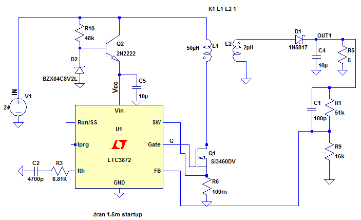
Figure 10
It is worth noting that the ratio of inductances on a transformer is equal to the square of the turns ratio. Thus the transformer above has an inductance ratio of 25:1, giving a turns ratio of 5:1.
Also, if n inductors of the same value and wound on the same core are placed in series, the combined inductance is n squared x the value of a single inductor.
If the transformer datasheet specifies a leakage inductance, this can be modelled as an additional primary inductor, but this inductor is not included in the SPICE directive detailing the mutual inductance. Thus any energy in this leakage inductance is not coupled into the secondary winding during the flyback cycle and manifests itself as ringing.
Want to know more?
Please see LTspice Tutorial: Part 4
LTspice is a registered trademark of Analog Devices Inc
Sitemap: www.simonbramble.co.uk/sitemap
© Copyright Simon Bramble