Digital Control of a Power Supply
Digital Control of a Power Supply
Introduction
Any analogue power supply can be controlled digitally as long as the designer has access to the feedback pin. Figure 1 shows a typical buck regulator based on the LTC3864.
Introduction
Any analogue power supply can be controlled digitally as long as the designer has access to the feedback pin. Figure 1 shows a typical buck regulator based on the LTC3864.
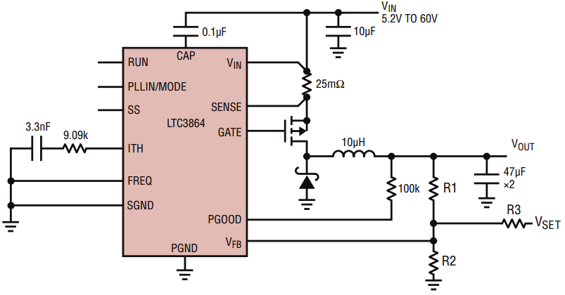
Figure 1
Normally the output voltage is set using two feedback resistors, R1 and R2 and the chip regulates the output voltage to keep the junction of these two resistors at a set voltage. In the case of the LTC3864 it is 0.8V.
An additional voltage (say, from a DAC) can be used to pull the feedback pin up and down to thus adjust the output voltage. A design example is shown below.
To Design a Digitally Adjustable Power Supply with Vout Ranging from 5V to 15V
We are going to calculate the feedback resistors needed to adjust the output voltage of the above power supply from 5V to 15V using a DAC with an output voltage from 0V to 3v3.
It can be seen that when the DAC voltage is high, the FB pin will be pulled high, so the chip will compensate by reducing the output voltage. Likewise when the DAC voltage is low, the FB pin will be pulled down, so the output voltage will rise. Thus the DAC output voltage is in antiphase with the power supply output voltage.
Summing the currents into the FB node, we can see that the current flowing down R1 added to the current flowing from VSET through R3 is equal to the current flowing in R2, since no current flows into the FB pin.
Thus:
VFB = 0.8V.
When the DAC output is 3v3, the output voltage needs to be 5V, thus
Let R2 = 10k
When the DAC output is 0V, the output voltage needs to be 15V, thus
Equating the above two equations gives
so
so
so
Putting this back into equation 1 gives
So R3 = 48.576k
So R1 = 147.187k
It is worth putting these values back into the original two equations to make sure they balance.
Once the calculations are correct, select preferred resistor values closest to the calculated values. If R3 is lowered, the DAC voltage will have more influence over the feedback voltage meaning VDAC will not have to rise to 3v3 to achieve 5V or go down to 0V to achieve 15V. The simulations shows the output voltage starting at 15.0V and decaying to 4.7V since the value for R3 is 47k and not the 48.5k we calculated. Either make up 48.576k using other resistors or write the software to ensure the DAC voltage goes not go up to 3v3.
An LTspice simulation demonstrating this is shown in Figure 2.
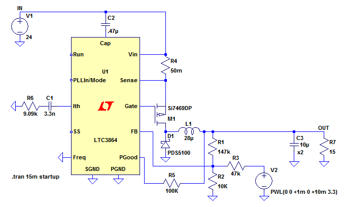
Figure 2
Complete IC based solutions for implementing digital control of power supplies are provided by Analog Devices. Please refer to: LTC2974, LTC2977, LTC3883, LTC3880, LTM4676, LTM2987:
The circuit of Figure 2 can be downloaded here:
LTspice is a registered trademark of Analog Devices Inc
Sitemap: www.simonbramble.co.uk/sitemap
© Copyright Simon Bramble